


16 bit accelerometer with Bi2C interface
The Bi2C – ACC (16 bit accelerometer) is our first product in our Bi2C series I2C expansion modules. You can read more about the Bi2C concept here.
This modules is based around the Industry standard Memsic MC3419 accelerometer.
We’ve also used this accelerometer on our Challenger RP2040 WiFi/BLE board.
The MC3419 is a small form factor, integrated digital output 3-axis accelerometer with a feature set optimized for cell phones and consumer product motion sensing. Applications include user interface control, gaming motion input, electronic compass tilt compensation for cell phones, game controllers, remote controls and portable media products. The MC3419 features a dedicated motion block which implements algorithms to support “any motion” and shake detection, tilt/flip and tilt 35 position detection. Low power consumption and small size are inherent in the monolithic fabrication approach, where the MEMS accelerometer is integrated in a single-chip with the electronics integrated circuit. In the MC3419 the internal sample rate can be set from 0.5 to 2000 samples / second. The MC3419 supports the reading of sample and event status via polling or interrupts.
Some of its features broken down are:
- ±2, ±4, ±8, ±12, ±16g range
- 16-bit single sample resolution
- 16-bit resolution with FIFO
- 0.5 to 2000 Hz Output Data Rate
- 4μA typical Standby current – making it an ideal companion to our Challenger 840 BLE boards
- Low typical active current
- I²C interface, up to 1 MHz
This Bi2C module is only 10mm * 12mm and is meant to be mounted with a strong double sided tape or glued into place.
It is shipped with one 5cm long flexible flat cable so that you can plug it straight in to your Challenger board.
The module has true I2C daisy chaining capabilities which means you can connect as many Bi2C modules in one chain as you like. Or at least as many as can reliably work on the same I2C bus.
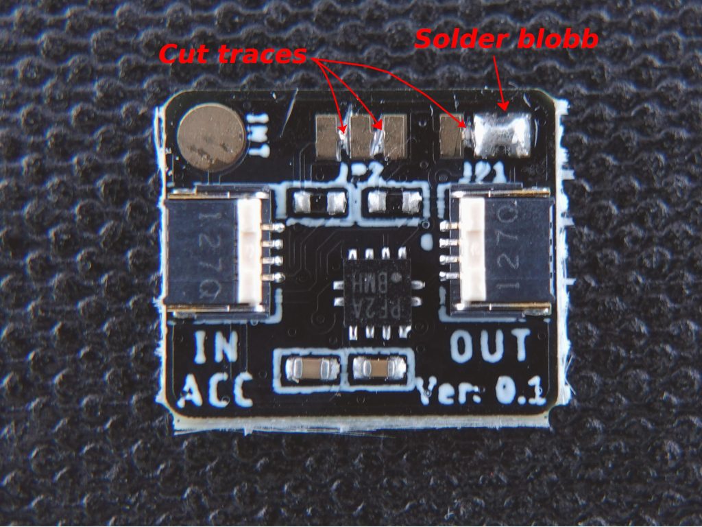
You also have the possibility to fully disable the pull up resistors on the module by cutting the wire links on JP2. There should only be one device in the Bi2C chain that have the pull up resistors enabled. All the other devices must have them disabled.
If you need to connect another Bi2C – ACC device on the same Bi2C bus you also have the possibility to configure the accelerometer to its second I2C address (0x6C). This is done by cutting the wire link on JP1 and creating a solder blobb on the other two pads on the board.
Below is a picture showing a Bi2C – ACC sensor with pull up resistors disabled and its I2C address reconfigured for 0x6C.


Reviews
There are no reviews yet.